シリコン・ネクサス:戦略的競争時代における世界のAI半導体事情の解読
エグゼクティブサマリー
世界の半導体産業は、生成AIの爆発的な需要を原動力とする歴史的な転換点に立っている。本レポートは、この変革の中心にあるAI半導体をめぐる技術、市場、地政学の複雑な相互作用を詳細に分析するものである。市場は、生成AIの普及により前例のない成長を遂げており、データセンターへの巨額投資が続いている。この潮流の中で、NVIDIAはその高性能GPUと成熟したCUDAソフトウェアエコシステムによって圧倒的な支配的地位を築いているが、その牙城は多方面からの挑戦に晒されている。
第一に、ハイパースケールクラウド事業者(Google、Amazon、Microsoft)は、コスト削減、性能最適化、サプライチェーン管理の強化を目的として、独自のカスタムシリコン(ASIC)開発を加速させている。第二に、Cerebras、SambaNova、Groqといった革新的なスタートアップ企業が、従来のアーキテクチャの限界を打破する斬新なアプローチで、特定領域における性能の桁違いの向上を実現し、新たな市場を切り拓いている。
同時に、米中間の技術覇権争いを軸とした地政学的対立は、グローバルなサプライチェーンの「分断化(Bifurcation)」を不可逆的に進行させている。米国の輸出規制は中国の最先端技術へのアクセスを制限する一方、中国国内の半導体自給自足に向けた国家的な取り組みを強力に後押ししている。これに対し、日本、欧州連合(EU)、韓国、台湾といった主要経済圏も、巨額の公的資金を投じて独自の半導体戦略を推進し、自国の技術主権と供給網の強靭化を図っている。
技術面では、「ムーアの法則」の物理的・経済的限界が明らかになる中、チップレットや3D積層といった先進パッケージング技術が性能向上の主要な牽引役となっている。次世代トランジスタ構造であるGate-All-Around(GAA)や、2nm以下の超微細プロセスノードへの移行は、AIコンピューティングの未来を左右する重要な技術的変曲点である。
本レポートは、これらの動向を包括的に分析し、技術企業、投資家、政策立案者といった主要なステークホルダーに対し、このダイナミックで不確実性の高い環境を乗り切るための戦略的な洞察と実用的な提言を提供する。
第1章 AIコンピューティングのアーキテクチャ基盤
本章では、AI半導体を支える基本的な技術原理を解説する。これらのチップが従来のものとどう違うのか、主要なアーキテクチャのアプローチ、そしてAIのワークロードや展開環境(データセンター対エッジ)に応じた適用方法について詳述する。
1.1 新しいコンピューティングクラスの定義:AIアクセラレータ
AI半導体、あるいはAIアクセラレータとは、機械学習やディープラーニングといったAI特有の数学的演算処理に最適化された半導体の総称である 1。従来の汎用的な中央処理装置(CPU)が逐次的なタスク処理に優れているのに対し、AIアクセラレータは、ニューラルネットワークで必要とされる膨大な行列演算やベクトル演算を効率的に処理するため、大規模な並列処理能力と高い演算密度を持つように設計されている 2。
この設計思想により、AIアクセラレータは従来のCPUと比較して、AIタスクにおいて劇的に高速な処理能力と、優れた電力効率(ワットあたりの性能)という2つの主要な利点を提供する 2。
1.2 アクセラレータの三つの潮流:GPU、ASIC、FPGA
AIアクセラレーションには、主に3つの異なるアーキテクチャが存在し、それぞれに固有のトレードオフがある。
- GPU(Graphics Processing Unit): もともとはグラフィックス描画用に開発されたが、数千個のコアを持つそのアーキテクチャが、ディープラーニングにおける並列計算に極めて適していることが判明した 2。この適応性の高さから、AIモデルの学習(トレーニング)や要求の厳しい推論(インファレンス)タスクにおける事実上の標準となっている 5。しかし、その汎用的な並列処理能力ゆえに、特定の固定化されたAIタスクにおいては、必ずしも最も電力効率の高いソリューションとは限らない 3。
- ASIC(Application-Specific Integrated Circuit): 特定用途向け集積回路であり、単一の目的のためにカスタム設計されたチップである。AIの文脈では、特定のニューラルネットワークやアルゴリズム群(例:Transformerモデル)をハードウェアレベルで実装し、最高の効率を達成することを意味する 2。この特化により、特定のタスクにおいて最高の性能と最小の消費電力を実現するが、柔軟性という代償を伴う。ASICは一度製造されると他のタスクに再プログラムすることはできず、初期の開発・製造コスト(NRE)が非常に高額になる 3。GoogleのTPU(Tensor Processing Unit)がその代表例である 12。
- FPGA(Field-Programmable Gate Array): 製造後でもユーザーが内部の論理回路を再構成できるという、中間の選択肢を提供する 13。これにより、ソフトウェアのような柔軟性を持ちながら、ハードウェアレベルの性能を発揮できる。AIアルゴリズムがまだ進化途上にあるアプリケーションや、極めて低い確定的レイテンシが要求されるタスクに最適である 11。特定のタスクにおいてはGPUよりも電力効率に優れるが、専用設計のASICほどのピーク性能は得られない 3。その再プログラム可能な性質から、後にASICとして製品化される設計のプロトタイピングにも適している 11。
これらのアーキテクチャの選択は、単純な優劣ではなく、ビジネスケースに依存する複雑な最適化問題である。研究開発段階では柔軟性の高いGPUが好まれ、大量生産されるコンシューマ製品ではコスト効率の高いASICが採用され、急速に進化する産業用アプリケーションでは再構成可能なFPGAが価値を発揮する。これは、各アーキテクチャが競合するだけでなく、製品ライフサイクルの異なる段階で互いに補完し合う関係にあることを示唆している。したがって、企業は単一のプラットフォーム戦略ではなく、AIハードウェアのポートフォリオ戦略を策定する必要がある。
表1:AIアクセラレータアーキテクチャの比較
| 項目 | GPU (Graphics Processing Unit) | ASIC (Application-Specific Integrated Circuit) | FPGA (Field-Programmable Gate Array) |
| 主要特性 | 数千のコアによる大規模並列処理 | 特定用途に特化したカスタム回路 | 製造後に再構成可能な論理ブロック |
| 主なAI用途 | モデルのトレーニング、高性能推論 | 特定モデルの大量推論(例:エッジデバイス) | 低レイテンシ推論、プロトタイピング、進化するアルゴリズム |
| 性能 | 高 | 最高(特定タスクにおいて) | 中~高 |
| 電力効率 | 中 | 最高 | 高 |
| 柔軟性・再プログラム性 | 高(ソフトウェアで対応) | 不可 | 最高(ハードウェアレベルで再構成可能) |
| 開発コスト (NRE) | 低 | 最高 | 中 |
| ユニットコスト(量産時) | 高 | 最低 | 中 |
| 市場投入までの時間 | 短 | 長 | 中 |
1.3 AIの両輪:トレーニングとインファレンスのワークロード
AIのワークロードは、ハードウェアに全く異なる要求を課す「トレーニング」と「インファレンス」という2つの主要なフェーズに大別される。
- トレーニング: 大量のデータセットをAIモデルに供給し、「学習」させるプロセス。膨大な計算能力(多くは32ビットや16ビットの浮動小数点演算精度を使用)、モデルとデータを保持するための大容量メモリ、そして数千のチップにまたがってスケールする能力が求められる。その圧倒的な性能とプログラマビリティから、歴史的にGPUがこの領域を支配してきた 5。
- インファレンス: 学習済みのモデルを使用して、新しいデータに対して予測を行うプロセス。多くの場合、低レイテンシ、高い電力効率(特にエッジデバイスにおいて)、そしてINT8のような低精度の演算処理能力が重要となる 5。データセンターでの高性能インファレンスにはGPUが使用されるが、特定の高ボリュームなタスクにおいては、その効率性からASICやFPGAがますます好まれるようになっている 6。
このトレーニングとインファレンスの要求仕様の乖離は、アーキテクチャの多様化を促進する主要な要因となっている。NVIDIAのGPUがトレーニング市場で築いた牙城は、インファレンス市場での成功を保証するものではない。インファレンス市場はより細分化されており、特にエッジ分野ではASICやFPGAベンダーにとって巨大な成長機会となっている。AIの総所有コスト(TCO)は、一度訓練されれば何十億回も使用されるモデルの性質上、トレーニングコストよりもインファレンスコストに大きく左右されるようになる。この経済的現実が、汎用GPUよりも超効率的なカスタムハードウェア(ASIC)へのシフトを後押ししている。
1.4 インテリジェンスの在り処:データセンターAI vs. エッジAI
AI処理が物理的にどこで行われるかは、半導体の設計を根本的に決定づける。
- データセンターAI: 大規模なトレーニングとインファレンスを特徴とする。ハードウェアはピーク性能に最適化され、チップあたり数百ワットという高い消費電力と高度な冷却システムを伴うことが多い。スループットと、最も複雑で巨大なモデルを実行する能力が重視される 3。
- エッジAI: スマートフォン、自動車、IoTセンサー、産業用ロボットなどのデバイス上で直接AIインファレンスを実行する 2。主な制約は、消費電力(ミリワット単位の場合もある)、物理的なサイズ、そしてコストである 21。エッジAIは、リアルタイムの応答を可能にし、データをローカルに保持することでプライバシーを強化し、クラウドへの接続依存度を低減する 2。この分野では、NPU(Neural Processing Unit)を統合した専用のSoC(System on a Chip)が一般的である 3。
第2章 AI半導体市場のランドスケープ:多方面にわたる競争の最前線
本章では、AI半導体市場の規模、成長性、そして競争構造を包括的に分析する。既存の支配的企業、独自のチップを開発するハイパースケールクラウド事業者、そして斬新なアーキテクチャで現状に挑戦する革新的なスタートアップという、3つの異なるグループに分類し、各プレイヤーの戦略を詳述する。
2.1 市場規模と成長軌道:前例のない成長スーパーサイクル
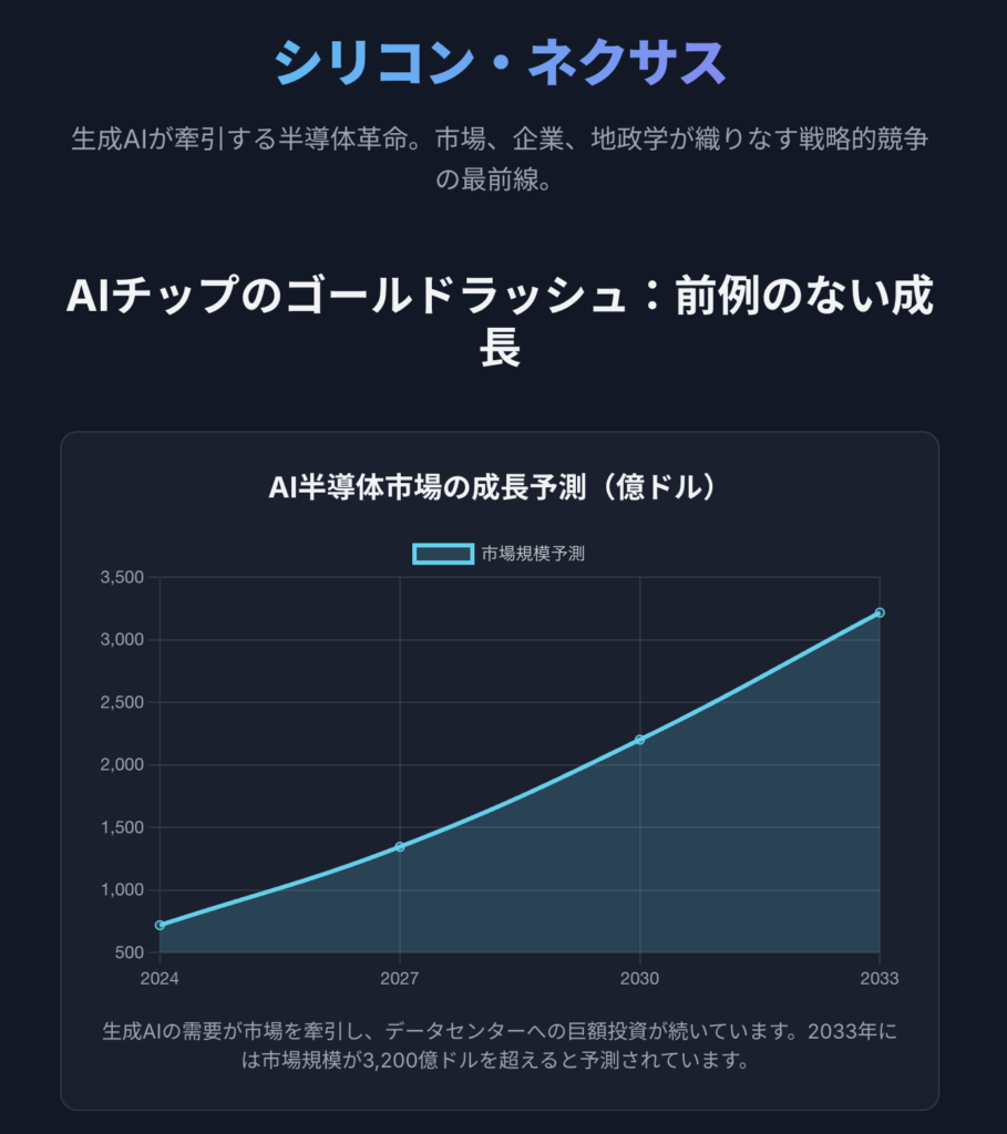
世界のAI半導体市場は、爆発的な成長期にある。ある調査では、2024年の719.1億米ドルから2033年には3,216.6億米ドルに達し、年平均成長率(CAGR)18.11%で成長すると予測されている 23。別の調査では、2025年の650.1億米ドルから2034年には2,328.5億米ドル(CAGR 15.23%)への成長が見込まれている 24。Gartner社は、AIを主要な牽引役として、2025年の半導体市場全体が7,170億米ドルに達すると予測している 25。この成長の主な原動力は、トレーニングとインファレンスの両方で膨大な計算能力を必要とする生成AIの需要であり、データセンターインフラへの前例のない投資を促している 7。
市場をアプリケーション別に分析すると、データセンターが最大かつ最も急速に成長しているセグメントであり、2030年までに約5,000億米ドルに達し、半導体業界全体の支出の半分以上を占めると予測されている 31。エッジAI市場も力強い成長を遂げており、コンシューマエレクトロニクス、自動車(ADAS)、産業用IoTに牽引され、2034年までに220億米ドルに達すると予測されている 33。特に車載半導体市場は、2023年の760億米ドルから2028年には1,170億米ドルに拡大すると見込まれている 36。
2.2 既存の支配者たち:牙城の防衛
- NVIDIA:
- 市場支配: NVIDIAはデータセンター向けAIチップ市場において65%から92%という圧倒的なシェアを誇り、議論の余地のないリーダーである 30。この支配力は同社の企業価値を記録的な水準に押し上げている 7。
- CUDAという「堀」: NVIDIAの最大の競争優位性は、ハードウェアそのものだけでなく、独自の並列コンピューティングプラットフォームであるCUDAにある 39。この成熟したソフトウェアエコシステムは、豊富なライブラリ(cuDNN、TensorRT)、開発ツール、広範なコミュニティサポートを提供し、強力なベンダーロックインと競合他社にとって高い参入障壁を生み出している 41。
- 製品ロードマップ: Hopper(H100/H200)からBlackwell(B100/B200/GB200)、そして発表済みのVera Rubinアーキテクチャへと続く、1年周期の積極的な製品投入は、世代ごとに指数関数的な性能向上を提供し、常に性能の限界を押し上げている 45。
- AMD (Advanced Micro Devices):
- 主要な挑戦者: AMDは、高性能GPU分野におけるNVIDIAの主要な対抗馬として位置づけられている。その戦略は、Instinctアクセラレータシリーズ(MI300X、MI325X、次期MI350シリーズ)で、特にメモリ容量と帯域幅において競争力のある性能を提供することに重点を置いている 49。
- ROCmエコシステム: AMDのオープンソースソフトウェアプラットフォームであるROCmは、CUDAの直接的な競合製品として設計されている。PyTorchやHugging Faceといった主要なフレームワークからのサポートを得て大幅に成熟したが、エコシステムの広さ、ドキュメントの質、開発者の採用率では依然としてCUDAに後れを取っている 51。AMDは、CUDAコードをROCmに移植するのに役立つHIPのようなツールを通じて、このギャップを埋めるべく積極的に取り組んでいる 53。
- 性能ベンチマーク: 最近のベンチマークでは、AMDのMI300Xが、特に大容量メモリの恩恵を受ける特定のLLMインファレンスワークロードにおいて、NVIDIAのH100と同等かそれ以上の性能を発揮することが示されている 51。
- Intel:
- 多角的な戦略: Intelは、独自のGPU(Ponte Vecchio、Falcon Shores)を開発する一方で、Habana Labsの買収を通じて特殊なASIC(Gaudiシリーズ)を提供するという二正面戦略を追求している 61。
- Gaudiアクセラレータ: Gaudiシリーズ(Gaudi 2、Gaudi 3)は、特にAIトレーニングにおいて、NVIDIA GPUに対する費用対効果の高い高性能な代替品として位置づけられている 63。しかし、Intelの戦略は焦点が定まっていないと批判されており、将来のGaudi世代の開発中止と新アーキテクチャJaguar Shoresへの転換につながった 61。
- ソフトウェアとエコシステム: Intelは、NVIDIAのロックインを打破することを目指し、ベンダーニュートラルなオープンソフトウェア標準としてoneAPIを推進しているが、その採用は依然として大きな課題である 44。
表2:主要AIデータセンターGPUの仕様比較
| 製品名 | アーキテクチャ | プロセスノード | メモリタイプ | メモリ容量 (GB) | メモリ帯域幅 (TB/s) | ピーク性能 (FP16/BF16) |
| NVIDIA H200 | Hopper | TSMC 4N | HBM3e | 141 | 4.8 | 989 TFLOPS |
| NVIDIA B200 | Blackwell | TSMC 4NP | HBM3e | 192 | 8.0 | 4.4 PFLOPS (2,200 TFLOPS) |
| AMD Instinct MI300X | CDNA 3 | 5/6nm Chiplet | HBM3 | 192 | 5.3 | 1.3 PFLOPS (1,300 TFLOPS) |
| AMD Instinct MI325X | CDNA 3 | 5/6nm Chiplet | HBM3e | 256 | 6.0 | 1.3 PFLOPS (1,307 TFLOPS) |
| Intel Gaudi 3 | Habana Goya | TSMC 5nm | HBM2e | 128 | 3.7 | 1.8 PFLOPS (1,835 TFLOPS) |
2.3 ハイパースケーラー:カスタムシリコンの台頭
クラウドサービスプロバイダー(CSP)は、AIチップを自社で設計するという戦略的転換を進めている。この「Build vs. Buy(内製か購入か)」の判断は、以下の3つの主要な動機に基づいている。1) コスト削減: NVIDIAの高い利益率を回避し、大規模運用におけるTCOを最適化する 67。2)
性能最適化: 自社の主要なワークロード(検索、レコメンデーション、LLMインファレンスなど)にハードウェアを特化させ、ワットあたりの性能を最大化する 67。3)
サプライチェーン管理: 単一サプライヤー(NVIDIA)への依存を減らし、供給の安定性を確保する 68。
- Google (TPU):
- カスタムAI ASICのパイオニア。初期のTPUから、最新世代のTrillium(TPU v6e)およびIronwood(TPU v6p)に至るまで、その進化は自社のソフトウェアスタック(TensorFlow, JAX)と深く統合されている 71。
- 性能分析によると、Trilliumは前世代比で4.7倍の性能向上を達成し、電力効率も67%改善されている 73。ベンチマークでは、特定のワークロードにおいてGPUよりも優れたコスト効率を示すことが報告されている 74。
- Amazon (AWS Trainium & Inferentia):
- AWSは2つのチップ戦略を採用している。コスト効率の高いモデルトレーニング用のTrainiumと、高性能・低コストのインファレンス用のInferentiaである 79。
- 例えば、Inferentia2は第一世代と比較して最大4倍のスループットと最大10倍の低レイテンシを実現し、同等のGPUインスタンスよりも最大40%優れた価格性能比を謳っている 79。この戦略は、AIワークロードにおいて魅力的なTCOを提供することで、顧客をAWSエコシステムに引き込むことを目的としている 67。
- AWS Neuron SDKは、PyTorchやTensorFlowなどのフレームワークとの統合を容易にするソフトウェアレイヤーを提供する 79。
- Microsoft (Azure Maia):
- Maia 100アクセラレータは、Microsoft初のカスタムAIチップであり、OpenAIのワークロード向けに共同設計された 86。
- その戦略は、TSMCの5nmプロセスから、ラック内のカスタム液体冷却システム、高帯域幅のイーサネットネットワーキングに至るまで、すべてをAzureインフラに最適化した完全な垂直統合アプローチである 87。これにより、Azure OpenAIやCopilotといった主要サービスに強力で最適化されたプラットフォームを提供している。
2.4 イノベーターたち:アーキテクチャの破壊
従来のGPU/ASICパラダイムに根本的な疑問を投げかけ、超低レイテンシや超大規模スケールといった特定のニッチ市場をターゲットとするスタートアップ企業が存在する。
- Cerebras Systems:
- ウエハースケール・エンジン(WSE): Cerebrasの独自アプローチは、シリコンウェハー全体を単一の巨大なチップとして利用することである(WSE-3は4兆個のトランジスタと90万個のコアを搭載) 93。
- このアーキテクチャは、従来のチップ間通信のボトルネックを解消し、巨大なオンチップメモリ帯域幅(21 PB/s)を提供することで、大規模モデルのトレーニングにおけるプログラミングモデルを単純化する 96。また、コンピューティングとメモリを分離することで、最大1.2ペタバイトの外部メモリへの拡張を可能にし、最大24兆パラメータのモデルに対応する 99。
- 最近のベンチマークでは、Llama 3.1-405Bのような大規模モデルにおいて、GPUベースのクラウドよりも最大75倍高速という記録的なインファレンス性能が示されている 101。
- SambaNova Systems:
- 再構成可能データフロー・アーキテクチャ(RDA): SambaNovaのアーキテクチャは、チップ内のデータフローを最適化することに重点を置いている。SambaFlowソフトウェアがAIモデルをデータフローグラフにコンパイルし、それを再構成可能データフロー・ユニット(RDU)上に空間的にプログラミングすることで、データ移動を最小限に抑え、ハードウェア使用率を最大化する 103。
- 最新チップSN40Lは、3層のメモリ階層を持ち、数百のモデルを保持してマイクロ秒単位で切り替えることができるため、エージェント型ワークフローや専門家混合(CoE)モデルに最適である 107。
- ベンチマークでは、単一の16チップノードが数百のGPUを上回る性能を大規模モデルで発揮し、Llama 3 8Bで毎秒1000トークン以上を達成したと報告されている 110。
- Groq:
- 言語処理ユニット(LPU): Groqのアーキテクチャは、超低レイテンシのAIインファレンスという唯一の目的のために構築されている 114。外部メモリを持たず(すべてオンチップSRAM)、ソフトウェアによって決定論的にスケジュールされる設計を採用することで、GPUのボトルネックと性能のばらつきを排除している 116。
- このアプローチは、リアルタイムの対話型AIやエージェントシステムなど、即時応答が不可欠なシングルストリームのアプリケーションにおいて比類のない速度を提供する 120。大規模モデルを保持するには多数のチップをネットワーク接続する必要があるが、ユーザー一人当たりの性能は革命的である 116。
この競争環境は、単なるNVIDIAとAMDの二元対立ではない。それは、3つの階層からなる複雑なチェス盤のようなものである。**第1層(既存の支配者)**は、NVIDIAを筆頭に、強力なハードウェアとソフトウェアの「堀」(CUDA)によって現在を支配している。**第2層(ハイパースケーラー)**は、垂直統合を活用して独自の閉鎖的なエコシステムを構築し、クラウド特化型AIの未来を築いている。**第3層(イノベーター)**は、第1層のアーキテクチャの基本的前提を攻撃し、ニッチでありながら将来的に巨大化する可能性のある市場(Groqのリアルタイムエージェント、Cerebrasの超大規模トレーニングなど)を狙っている。
この構造から導き出されるのは、NVIDIAにとっての長期的な最大の脅威は、AMDのような別のGPU企業ではなく、ハイパースケーラーによる需要の内製化と、イノベーターによるGPUが最適解ではない新たなコンピューティングカテゴリの創出という複合的な影響である、ということだ。さらに、この戦いの真の戦場はハードウェア性能そのものではなく、ソフトウェアエコシステムである。NVIDIAのCUDAは、莫大な乗り換えコストを生み出す最も手ごわい競争優位性である 41。すべての競合他社はこの事実を理解しており、AMDの成功はROCmの成熟にかかっている 51。このため、AIハードウェアの競争は、シリコン戦略と同等かそれ以上に、ソフトウェア戦略、特に開発者コミュニティを育成するオープンソース戦略の巧拙によって決まるだろう。
表3:革新的AIアクセラレータの比較分析
| 企業名 | コアアーキテクチャ | 主要な差別化要因 | ターゲットワークロード | 主要性能指標 |
| Cerebras Systems | ウエハースケール・エンジン (WSE) | ウェハー全体を単一チップとして使用し、チップ間通信を排除 | 超大規模モデルのトレーニングと推論 | パラメータ数(最大24兆)、メモリ帯域幅(21 PB/s) |
| SambaNova Systems | 再構成可能データフロー・アーキテクチャ (RDA) | データフローを最適化し、データ移動を最小化。複数モデルを同時保持可能 | 複雑な推論、専門家混合(CoE)モデル、エージェント型ワークフロー | 複数モデルの切り替え速度(マイクロ秒)、大規模モデルでのt/s/ユーザー |
| Groq | 言語処理ユニット (LPU) | 決定論的・ソフトウェアスケジュールによる超低レイテンシ | リアルタイム・シングルストリーム推論、対話型AI | 最初のトークンまでの時間(TTFT)、ユーザーあたりのt/s |
第3章 地政学的スーパーサイクル:国家戦略とサプライチェーンの再編
本章では、地政学がAI半導体産業に与える強力な影響を検証する。激化する米中間の「チップ戦争」、そして日本、EU、韓国、台湾といった他の主要経済圏による戦略的対応と、それに伴うグローバルサプライチェーンの分断化について詳述する。
3.1 チップ戦争:米国の輸出規制と中国の対応
- 米国の戦略: 2022年10月に米国商務省産業安全保障局(BIS)によって導入され、その後強化された輸出規制は、中国が高性能AIチップおよびその製造に必要な装置を入手することを制限し、軍事近代化とAI開発を遅らせることを明確な目的としている 123。規制は「総処理性能(TPP)」や「性能密度」といった特定の技術的指標を用いて対象となるチップを定義しており、NVIDIAやAMDのような企業に複雑なコンプライアンス上の課題を突きつけている 127。これにより、NVIDIAは中国向けに性能を落とした輸出準拠モデル(H20など)を開発し、米国政府との複雑な交渉を余儀なくされ、数十億ドル規模の潜在的な売上を失った 130。
- 中国の自給自足戦略: これに対し、中国は半導体産業の国内育成を国家安全保障上の最優先事項と位置づけ、その取り組みを劇的に加速させている 137。
- 「大基金」: 国家集積回路産業投資基金は現在第3期に入り、475億米ドル規模の資金を設計から製造、素材に至るサプライチェーンのあらゆるセグメントに投入している 140。
- 国内チャンピオンの育成: Huaweiが「国家チャンピオン」として台頭し、同社のAscend AIチップ(例:910B)は、NVIDIA製品の代替としてBaiduやTencentといった他の中国IT大手に採用され始めている 144。Ascend 910Bは、NVIDIAの旧世代のA100 GPUに匹敵する性能を持つと評価されている 148。
- 製造技術の進展: SMIC(中芯国際集成電路製造)は、旧式のDUV(深紫外線)露光装置を使用しながらも7nmプロセスの開発に成功し、制裁下でも技術革新が可能であることを示したが、依然として最先端からは数世代遅れている 152。
- 新興スタートアップ: CambriconやBiren TechnologyなどのAIチップスタートアップも政府の支援を受けているが、米国の制裁や厳しい競争に直面している 137。
この米国の輸出規制は、短期的には中国の最先端AIハードウェアへのアクセスを遅らせることに成功しているが、同時に中国国内の半導体産業にとってこれ以上ない強力な触媒として機能しているという、両刃の剣の側面を持つ。保護された国内市場と国家安全保障という至上命令によって、中国の巨大IT企業はNVIDIAから離れ、Huaweiのような国内チャンピオンを育成せざるを得なくなっている。これは、HuaweiがNVIDIAとの自由競争では決して得られなかったであろう収益、規模、そして実世界からのフィードバックループを獲得する機会を与えている。その結果、5年から10年後には、米国はこれまで以上に手ごわく、完全に独立した中国のAIハードウェア・ソフトウェアエコシステムに直面する可能性がある。
3.2 世界の対応:自国での能力構築
米中対立とパンデミックによって露呈したサプライチェーンの脆弱性を受け、他の主要経済大国も独自の野心的な産業政策を打ち出している。
- 日本の半導体ルネサンス: 1) TSMCの熊本工場(JASM)誘致によるレガシーチップ生産の確保、2) IBMとの提携によるコンソーシアムRapidusを通じた次世代2nm技術の開発、3) 将来技術の研究開発、という三本柱の戦略を推進している 161。政府は2021年から2023年にかけて3.9兆円もの巨額の補助金を投じ、2027年までの2nm量産開始を目指している 161。
- 欧州連合のチップス法: 2030年までに世界の半導体市場におけるEUのシェアを現在の10%から20%に倍増させることを目指す、430億ユーロ規模のイニシアチブ 167。研究開発とパイロットラインの支援(Chips for Europe Initiative)、製造施設への投資誘致、そして将来の供給不足に備える危機対応メカニズムの構築という3つの柱で構成されている 167。
- 韓国のK-半導体戦略: 2030年までに自給自足型の「K-半導体ベルト」を構築するための4,500億米ドル規模の巨大計画であり、SamsungとSK Hynixという自国のチャンピオン企業の優位性をさらに強化するものである 173。AIアクセラレータに不可欠な広帯域幅メモリ(HBM)におけるリーダーシップを維持しつつ、先端ファウンドリサービス(2nmプロセス)やパッケージング分野への進出を強力に推進している。SK HynixとSamsungは、世界のHBM市場の50%以上を占めている 173。
- 台湾の「シリコンの盾」: 台湾の戦略は、世界の最先端チップの90%以上を生産するTSMCの技術的優位性を維持することに集約される 177。この支配力は、台湾を世界経済にとって不可欠な存在にし、軍事紛争を抑止する理論上の「シリコンの盾」として機能している 178。しかし、この一極集中は同時に巨大な地政学的リスクでもあり、米国や日本などの同盟国はTSMCに海外での製造拠点の多様化を促している 178。
これらの国家戦略は、単に製造工場を自国内に誘致するだけでなく、サプライチェーンにおける重要な「チョークポイント(隘路)」を確保するための戦略的な取り組みである。日本は素材・製造装置、韓国はHBM、米国は先進パッケージングといった、各国が自国の強みを持つ分野に重点的に投資している。これは、完全に自給自足の島々を作るのではなく、地政学的なライバルからの供給途絶に対して強靭な、同盟国間でコントロールされたチョークポイントのネットワークを構築しようとする動きであり、「グローバル化」から「フレンド・ショアリング」への移行を示している。
表4:各国の半導体戦略の概要
| 地域/国 | 主要政策イニシアチブ | 主な目標 | 投資規模(公的/民間) | 主要企業/コンソーシアム | 戦略的重点分野 |
| 米国 | CHIPS and Science Act | 国内製造能力の強化、研究開発の促進 | 527億米ドル(公的)+民間投資 | Intel, Micron, TSMC, Samsung | 最先端ロジック、先進パッケージング |
| 中国 | 大基金 (Big Fund) | 半導体の自給自足、技術的独立 | 475億米ドル(第3期)+地方政府資金 | SMIC, Huawei, YMTC, Cambricon | サプライチェーン全体の国産化 |
| 日本 | 半導体・デジタル産業戦略 | 国内製造基盤の再構築、次世代技術開発 | 3.9兆円(2021-23年)+民間投資 | Rapidus, JASM (TSMC), Kioxia | 2nmロジック、素材、製造装置 |
| EU | European Chips Act | 世界市場シェア倍増(20%へ)、供給網強靭化 | 430億ユーロ(官民) | STMicroelectronics, Infineon, Intel | 最先端製造、設計エコシステム |
| 韓国 | K-半導体戦略 | メモリ半導体支配の維持、システム半導体育成 | 4,500億米ドル(官民) | Samsung, SK Hynix | HBM、先端メモリ、ファウンドリ |
| 台湾 | – (TSMC中心) | 技術的リーダーシップの維持(シリコンの盾) | – (企業主導) | TSMC, MediaTek, UMC | 最先端ファウンドリ製造 |
3.3 分断化するサプライチェーン:二つの標準の世界へ?
これらの地政学的動向の長期的な帰結として、グローバルで高度に専門化されたサプライチェーンは、米国とその同盟国を中心とする領域と、中国を中心とする領域の2つに徐々に分断されつつある 182。この分断化は、技術的なデカップリング、別々の標準(例:CUDA対中国の国内ソフトウェア)、冗長なサプライチェーン、そして最終的には消費者にとってのコスト増といったリスクを生み出す 184。しかし、米国企業の中国市場への依存や、中国の外国製装置・素材への依存といった深い経済的相互関係が、完全かつ急速な分離を困難にしており、結果として、不完全で、徐々に進行し、浸透性のある乖離が進んでいる 183。
第4章 次なるフロンティア:技術的変曲点と将来展望
本章では、現在の状況を超え、次世代のAI半導体を定義するであろう主要な技術的シフトに焦点を当てる。パッケージングによる「ムーアの法則の先へ」の動き、トランジスタ自体の進化、より微細なプロセスノードへの競争、そして全く新しいコンピューティングパラダイムを探る。
4.1 ムーアの法則の先へ:先進パッケージングの時代
伝統的なトランジスタの微細化(ムーアの法則)が技術的・経済的に困難になるにつれて、業界は性能向上の主要な手段として先進パッケージング技術に注目している。これはしばしば「モア・ザン・ムーア」戦略と呼ばれる 187。
- チップレットとUCIe: 一つの大きなモノリシックなチップを製造する代わりに、より小さく特殊化された「チップレット」を単一のパッケージ内で接続してシステムを構築するアプローチが主流になっている 190。これにより、製造歩留まりが向上し、コストが削減され、異なるベンダーやプロセスノードのコンポーネントを組み合わせることが可能になる。**Universal Chiplet Interconnect Express (UCIe)**は、Intel、AMD、TSMC、Googleなどの業界大手が支援するオープンスタンダードであり、相互運用可能なチップレットエコシステムの創出を目指している 190。
- 3D積層とHBM: チップを垂直に積層する技術も性能を革命的に向上させている。その鍵となるのが**広帯域幅メモリ(HBM)**であり、DRAMチップを垂直に積み重ね、シリコンインターポーザを介してプロセッサに接続することで、データ集約型のAIアクセラレータに不可欠な巨大なメモリ帯域幅を提供する 191。この技術は、高密度な3Dスタックにおける熱管理といった新たな課題も生み出している 199。
モノリシックなスケーリングの終焉は、イノベーションのエコシステムを根本的に変えている。かつてはファウンドリ(TSMCなど)と設計者(NVIDIAなど)が中心であったが、チップレット時代には、インターコネクト(UCIe標準)、パッケージング、特殊IPブロックといった分野の専門企業が価値を創造するようになる。これにより、競争の主戦場はシリコン製造からシステムレベルの統合へと移行し、オープンスタンダードを定義するコンソーシアムが大きな力を持つことになるだろう。
4.2 トランジスタの未来:Gate-All-Around (GAA)
過去10年間の標準であったFinFETトランジスタアーキテクチャから、次世代の**Gate-All-Around(GAA)**アーキテクチャへの移行が進んでいる 201。GAAは、トランジスタのチャネルを四方からゲートで囲むことにより、優れた静電制御を実現し、3nm以下のさらなる微細化を可能にすると同時に、性能向上とリーク電力の低減をもたらす 202。しかし、GAAは原子レベルの精度での成膜やエッチングを必要とし、プロセス制御や静電気放電(ESD)保護において新たな製造上の複雑さを生み出している 202。
4.3 オングストロームへの競争:2nmおよび1.4nmプロセスのロードマップ
主要ファウンドリのプロセス技術ロードマップは、熾烈な競争を反映している。
- TSMC、Samsung、Intelは、いずれも2025年頃に2nmプロセスの量産開始を目指しており、これはTSMCにとってGAAトランジスタを商用化する最初のノードとなる(Samsungは3nmで既に導入済み) 205。
- 日本のRapidusは、2027年までに2nmの量産を開始するという野心的な目標を掲げている 205。
- さらにその先を見据え、各社は2027年から2028年頃の生産を目指して1.4nm(A14としても知られる)プロセスの開発計画を進めており、これによりさらなる性能向上と電力効率の改善が期待される 205。
4.4 新たなパラダイム:脳型および光速コンピューティング
現在研究段階にある、長期的には革命をもたらす可能性のあるコンピューティングアーキテクチャも存在する。
- ニューロモーフィック・コンピューティング: 人間の脳のアーキテクチャと機能を模倣し、「スパイキング・ニューラル・ネットワーク(SNN)」とイベント駆動型処理を用いて、極めて高いエネルギー効率を達成するアプローチ 211。
IntelのLoihi 2(11.5億ニューロンの「Hala Point」システムを駆動)、IBMのNorthPole、BrainChipのAkidaといった主要な研究プラットフォームの開発が進められている 211。 - 光電融合技術: チップ内およびチップ間のデータ伝送に、電子の代わりに光(光子)を利用する技術。これにより、従来の電気配線の帯域幅と消費電力のボトルネックを克服することが期待される 219。**NTTのIOWN(Innovative Optical and Wireless Network)**構想は、将来のデータセンターや通信インフラ向けに「オールフォトニクス・ネットワーク」を構築することを目指す主要な取り組みである 221。
これらの未来志向の技術は、すべて根本的な課題、すなわち電力問題の解決を目指している。AIモデルが大規模化するにつれて、データセンターのエネルギー消費と熱出力が主要な制約要因となっている 20。GAAトランジスタからニューロモーフィック、光コンピューティングに至るまで、将来のアーキテクチャはすべて、電力効率の飛躍的な向上を目的としている。これにより、AIハードウェアの最も重要な評価指標は、ピーク性能(FLOPS)から「ワットあたりの性能」へと移行するだろう。この変化は、液体冷却や新たな電力供給網といったデータセンター自体の根本的な再設計を促し、エネルギー効率の高いコンピューティングでリードする企業に決定的な経済的・環境的優位性をもたらす。
第5章 戦略的分析と提言
本章では、レポート全体の分析結果を統合し、AI半導体ランドスケープの全体像を提示する。未来を見据えた分析と、主要なステークホルダーに対する実行可能な提言を行う。
5.1 主要トレンドの統合:技術、市場、政治の合流
AI半導体産業は、以下の3つの力が合流する歴史的な変曲点にある。
- 技術的シフト: モノリシックな微細化からヘテロジニアスな統合へ。
- 市場のシフト: GPU一強時代から、多様な特殊アクセラレータが共存する時代へ。
- 地政学的シフト: グローバリゼーションから、国家の戦略的利益を優先する産業政策へ。
これらの力が相互に作用し合うことで、技術ロードマップが輸出規制に影響され、市場シェアが政府の補助金によって形成されるという、非常にダイナミックで不確実な環境が生まれている。
5.2 AIコンピューティングの未来:ヘテロジニアスで断片化されたランドスケープ
AIコンピューティングの未来は、単一のアーキテクチャに支配されるのではなく、異なるタスクに最適化された多様なハードウェアソリューションが共存するヘテロジニアスなエコシステムとなることが予測される。
- データセンター: 汎用的なトレーニング用の高性能GPU、ハイパースケーラーのクラウド内でのTCOに最適化されたカスタムASIC、そして超大規模ワークロード向けの斬新なアクセラレータ(ウエハースケールやデータフローシステムなど)が混在する 159。
- エッジ: 自動車、コンシューマエレクトロニクス、産業用IoTの特定用途向けに、SoCに統合された低消費電力のASICやNPUが急増する。
- ソフトウェアレイヤー: この異種混合のハードウェアを連携させるためのオープンおよびプロプライエタリなソフトウェアプラットフォーム(CUDA、ROCm、oneAPIなど)が決定的に重要な役割を果たし、開発者の支持をめぐる争いが続く 44。
5.3 ステークホルダーへの提言
- テクノロジー企業(チップ設計者・システムビルダー)へ:
- ヘテロジニアス性を受け入れる: 単一のソリューションに賭けるのではなく、異なるアーキテクチャを含むポートフォリオアプローチを開発する。
- ソフトウェアとオープンスタンダードへの投資: 強力なソフトウェアエコシステムは、ハードウェア性能単体よりも持続的な競争優位性となる。将来の相互運用性を確保するため、UCIeのような標準化団体に参加する。
- 地政学的リスクを乗り切る: 単一の供給拠点への依存を避け、サプライチェーンを多様化する。輸出規制を遵守しつつ収益損失を緩和するため、地域別の製品戦略を策定する。
- 投資家(VC、公開市場アナリスト)へ:
- 既存の支配者以外にも目を向ける: NVIDIAの地位は強固だが、エコシステム内の主要なボトルネック(先進パッケージング、インターコネクト、特殊インファレンスなど)を解決する企業によって大きな価値が創造されるだろう。
- 「ソフトウェアの堀」を評価する: 挑戦者を評価する際は、ハードウェアのベンチマークと同じくらい厳格に、そのソフトウェア戦略とコミュニティの採用状況を精査する。ソフトウェアのない優れたチップは、失敗した投資である。
- 地政学的シナリオを織り込む: 貿易制限の激化、サプライチェーンの混乱(特に台湾関連)、各国の産業政策の成否がポートフォリオ企業に与える影響をモデル化する。
- 政策立案者へ:
- 完全なエコシステムアプローチを育成する: 補助金は製造工場(ファブ)だけでなく、素材、EDAツール、先進パッケージングの研究開発、そして熟練した労働力といった、産業の「ロングテール」も支援する必要がある 228。
- 安全保障とイノベーションのバランスを取る: 敵対国への重要な能力の流出を防ぎつつ、国内企業の研究開発リーダーシップを支える収益とグローバル市場へのアクセスを損なわないよう、的を絞った「小さな庭と高い塀」方式の輸出規制を策定する 230。
- 国際協力を促進する: 中国以外の強靭な半導体エコシステムを構築し、共通の標準を推進するため、同盟国(例:装置における日米蘭、製造における日米韓台)との研究開発およびサプライチェーンにおける連携を強化する 162。
引用文献
- aconnect.stockmark.co.jp https://aconnect.stockmark.co.jp/coevo/ai-semiconductor/#:~:text=AI%E5%8D%8A%E5%B0%8E%E4%BD%93%E3%81%A8%E3%81%AF%E3%80%81%E6%A9%9F%E6%A2%B0,%E3%81%8C%E6%96%BD%E3%81%95%E3%82%8C%E3%81%A6%E3%81%84%E3%82%8B%E3%80%82
- AI半導体とは? データセンターの電力課題と革新的アプローチ … https://www.rapidus.inc/tech/te0003/
- AI半導体とは?種類やGPUとの違い、メリット・デメリットや日本 … https://www.witc.co.jp/blog/1r488jyrqa/
- 次世代AI半導体の革新を担うのは誰か? | PwC Japanグループ https://www.pwc.com/jp/ja/knowledge/thoughtleadership/next-wave-of-ai-semiconductor.html
- What is a GPU & Its Importance for AI | Google Cloud https://cloud.google.com/discover/gpu-for-ai
- AI半導体とは?生成AIの関係や役割、半導体企業や銘柄を紹介 – Jitera https://jitera.com/ja/insights/54120
- エヌビディアがけん引するAI半導体市場の今後 重要な役割を果たす日本企業は https://www.nomura.co.jp/wealthstyle/article/0201/
- プロセッサの基礎知識(2)~種類と使われ方~ – パナソニック – Panasonic https://industrial.panasonic.com/jp/ds/ss/technical/b21
- What are ASIC Chips? A Detailed Comparison with GPUs and Application Scenarios https://ai-stack.ai/en/asic-vs-gpu
- ASIC・FPGAとは?その違いと置き換え(ASIC化)・転換の方法と … https://www.epson.jp/prod/semicon/products/asic/about_asic1.htm
- FPGAとは?メリットや注目される理由もわかりやすく解説 – NECソリューションイノベータ https://www.nec-solutioninnovators.co.jp/sl/emb/column/04/index.html
- AI半導体の最新動向 ~ポストGPU時代の注目技術~ – 日本総研 https://www.jri.co.jp/file/advanced/advanced-technology/pdf/15918.pdf
- FPGA Artificial Intelligence (AI) Design | FPGA AI Projects – Promwad https://promwad.com/services/embedded/fpga-design/ai
- AI Acceleration Solutions | Altera FPGAs from Cloud to Edge https://www.altera.com/fpga-solutions/ai
- AI Acceleration Solutions | Altera FPGAs from Cloud to Edge https://www.intel.co.jp/content/www/jp/ja/fpga-solutions/artificial-intelligence/fpga-gpu.html
- [FPGA & AI] What is the current industry state – Reddit https://www.reddit.com/r/FPGA/comments/1esr8z9/fpga_ai_what_is_the_current_industry_state/
- FPGA Prototyping for Faster Validation and Production – Fidus Systems https://fidus.com/blog/fpga-prototyping-faster-validation-production/
- ASICs for AI on the rise at GPUs’ expense … – eeNews Europe https://www.eenewseurope.com/en/asics-for-ai-on-the-rise-at-gpus-expense/
- Can ASICs Overtake NVIDIA in AI Inference? | by Aron Brand – Generative AI https://generativeai.pub/can-asics-overtake-nvidia-in-ai-inference-9fb82d4f3d77
- Generative AI: The next S-curve for the semiconductor industry? – McKinsey https://www.mckinsey.com/industries/semiconductors/our-insights/generative-ai-the-next-s-curve-for-the-semiconductor-industry
- 「次世代デジタルインフラの構築」 に関する国内外の動向 https://www.meti.go.jp/shingikai/sankoshin/green_innovation/industrial_restructuring/pdf/023_04_00.pdf
- エッジAIで高性能と低消費電力をどのように両立するか? | Renesas ルネサス https://www.renesas.com/ja/blogs/enable-high-performance-low-power-inference-your-edge-ai-applications
- 半導体市場における人工知能(AI)は2033年までに市場規模3216億6000万米ドルを超えると予測 | NEWSCAST https://newscast.jp/news/2819941
- Artificial Intelligence (AI) in Semiconductor Market Size to Hit USD 232.85 Bn by 2034 https://www.precedenceresearch.com/artificial-intelligence-in-semiconductor-market
- Semiconductor Revenue To Grow 14% In 2025: Gartner – DCPost MEA https://www.dcpostmea.com/2024/10/semiconductor-revenue-grow-14-2025-gartner/
- Gartner sees double-digit semi growth ahead, mainly thanks to AI – Bits&Chips https://bits-chips.com/article/gartner-sees-double-digit-semi-growth-ahead-mainly-thanks-to-ai/
- Global semiconductor revenue to grow 14% in 2025 – Evertiq https://evertiq.com/news/56674
- Gartner Forecasts Strong Semiconductor Market Recovery Driven by AI, Memory, and GPU Growth – AnySilicon https://anysilicon.com/gartner-forecasts-strong-semiconductor-market-recovery-driven-by-ai-memory-and-gpu-growth/
- Planning for the future: 2025 semiconductor market outlook – Sourceability https://sourceability.com/post/planning-for-the-future-2025-semiconductor-market-outlook
- The AI Infrastructure Spending Binge: A High-Conviction Opportunity in Semiconductors and Datacenter Equipment Suppliers – AInvest https://www.ainvest.com/news/ai-infrastructure-spending-binge-high-conviction-opportunity-semiconductors-datacenter-equipment-suppliers-2508/
- 2030 Data Center AI Chip Winners: The Trillion Dollar Club – Semiconductor Engineering https://semiengineering.com/2030-data-center-ai-chip-winners-the-trillion-dollar-club/
- Data Center Semiconductor Trends 2025: Artificial Intelligence Reshapes Compute and Memory Markets – Edge AI and Vision Alliance https://www.edge-ai-vision.com/2025/08/data-center-semiconductor-trends-2025-artificial-intelligence-reshapes-compute-and-memory-markets/
- AI Chips for Edge Applications 2024-2034: Artificial Intelligence at the Edge – IDTechEx https://www.idtechex.com/en/research-report/ai-chips-for-edge-applications/956
- Edge AI Market Size, Share, Growth & Global Report [2032] – Fortune Business Insights https://www.fortunebusinessinsights.com/edge-ai-market-107023
- Edge AI Chips Market Size, Trends, Share & Growth Report 2030 – Mordor Intelligence https://www.mordorintelligence.com/industry-reports/edge-artificia-intelligence-chips-market
- 半導体産業の現状 | PwC Japanグループ https://www.pwc.com/jp/ja/knowledge/thoughtleadership/state-of-the-semicon-industry.html
- Nvidia: Maintaining Dominance in AI Chip Market – AInvest https://www.ainvest.com/news/nvidia-maintaining-dominance-ai-chip-market-2507/
- Data-Center AI Chip Market – Q1 2024 Update | TechInsights https://www.techinsights.com/blog/data-center-ai-chip-market-q1-2024-update
- CUDA Zone – Library of Resources – NVIDIA Developer https://developer.nvidia.com/cuda-zone
- CUDA – Wikipedia https://en.wikipedia.org/wiki/CUDA
- NVIDIA’s Winning Platform Strategy with CUDA – Digital Innovation and Transformation https://d3.harvard.edu/platform-digit/submission/nvidias-winning-platform-strategy-with-cuda/
- Why’s Nvidia such a beast? It’s that CUDA thing. – SemiWiki https://semiwiki.com/forum/threads/why%E2%80%99s-nvidia-such-a-beast-it%E2%80%99s-that-cuda-thing.21393/
- CUDA Refresher: The GPU Computing Ecosystem | NVIDIA Technical Blog https://developer.nvidia.com/blog/cuda-refresher-the-gpu-computing-ecosystem/
- How did CUDA succeed? (Democratizing AI Compute, Part 3) – Modular https://www.modular.com/blog/democratizing-ai-compute-part-3-how-did-cuda-succeed
- Top 10 NVIDIA GPUs for AI in 2025 – Atlantic.Net https://www.atlantic.net/gpu-server-hosting/top-10-nvidia-gpus-for-ai/
- GTC 2025 – Announcements and Live Updates – NVIDIA Blog https://blogs.nvidia.com/blog/nvidia-keynote-at-gtc-2025-ai-news-live-updates/
- Nvidia Draws GPU System Roadmap Out To 2028 – The Next Platform https://www.nextplatform.com/2025/03/19/nvidia-draws-gpu-system-roadmap-out-to-2028/
- NVIDIA GTC 2025: NVIDIA’s Roadmap for AI in Datacenter, Desktops, and Robots – Techsponential https://www.techsponential.com/reports/gtc2025
- AMD Instinct™ MI300 Series Accelerators https://www.amd.com/en/products/accelerators/instinct/mi300.html
- Introducing the AMD Instinct™ MI300 Series accelerators, Powering the Growth of AI and HPC at Scale https://www.amd.com/en/blogs/2023/introducing-the-amd-instinct-mi300-series-acceler.html
- AMD Accelerates Pace of Data Center AI Innovation and Leadership with Expanded AMD Instinct GPU Roadmap https://ir.amd.com/news-events/press-releases/detail/1201/amd-accelerates-pace-of-data-center-ai-innovation-and-leadership-with-expanded-amd-instinct-gpu-roadmap
- AMD Says MI300 Is Its ‘Fastest-Ramping Product,’ Teases New AI Chips ‘Later This Year’ https://www.crn.com/news/components-peripherals/2024/amd-says-mi300-is-its-fastest-ramping-product-teases-new-ai-chips-later-this-year
- A Comprehensive Guide: Switching from CUDA to ROCm – TensorWave https://tensorwave.com/blog/transitioning-to-high-performance-a-comprehensive-guide-to-switching-from-cuda-to-rocm
- ROCm vs CUDA: A Practical Comparison for AI Developers – SCIMUS https://thescimus.com/blog/rocm-vs-cuda-a-practical-comparison-for-ai-developers/
- ROCm vs Nvidia CUDA vs OpenCL #new #ai #shorts #amd – YouTube https://www.youtube.com/shorts/O7wh5kCMWG8
- CUDA v ROCm : r/AMD_Stock – Reddit https://www.reddit.com/r/AMD_Stock/comments/1hdqu6m/cuda_v_rocm/
- 5 REASONS TO CHOOSE THE AMD ROCm™ PLATFORM https://www.amd.com/content/dam/amd/en/documents/partner-hub/instinct/why-choose-rocm-platform.pdf
- [D] Why is CUDA so much faster than ROCm? : r/MachineLearning – Reddit https://www.reddit.com/r/MachineLearning/comments/1fa8vq5/d_why_is_cuda_so_much_faster_than_rocm/
- [D] ROCm vs CUDA : r/MachineLearning – Reddit https://www.reddit.com/r/MachineLearning/comments/wbdq5c/d_rocm_vs_cuda/
- ROCm vs CUDA: A Performance Showdown for Modern AI Workloads – TensorWave https://tensorwave.com/blog/rocm-vs-cuda-a-performance-showdown-for-modern-ai-workloads
- How Intel ruined an Israeli startup it bought for $2B—and lost the AI race | SemiWiki https://semiwiki.com/forum/threads/how-intel-ruined-an-israeli-startup-it-bought-for-2b%E2%80%94and-lost-the-ai-race.22062/
- “How Intel ruined an Israeli startup it bought for $2b, Habana Labs—and lost the AI race” (the end of the Gaudi chips) – Reddit https://www.reddit.com/r/mlscaling/comments/1ilp3q0/how_intel_ruined_an_israeli_startup_it_bought_for/
- 10 Top AI Chip Companies in 2025 – VKTR.com https://www.vktr.com/ai-market/10-top-ai-chip-companies/
- Habana® Gaudi2® AI Processor for Deep Learning Gets Even Better – Intel https://www.intel.com/content/www/us/en/developer/articles/technical/habana-gaudi2-processor-for-deep-learning.html
- The AI Chip Market Explosion: Key Stats on Nvidia, AMD, and Intel’s AI Dominance https://patentpc.com/blog/the-ai-chip-market-explosion-key-stats-on-nvidia-amd-and-intels-ai-dominance
- Exploring Alternative GPU Computing Platforms – SCIMUS https://thescimus.com/blog/alternative-gpu-computing-platforms-beyond-rocm-and-cuda/
- The Rise of Custom AI Chips: How Big Tech is Challenging NVIDIA’s Dominance | Aranca https://www.aranca.com/knowledge-library/articles/investment-research/the-rise-of-custom-ai-chips-how-big-tech-is-challenging-nvidias-dominance
- Embracing the Future: The Shift Towards Custom AI Chips in the AI Industry | by Debu Sinha https://medium.com/@debusinha2009/embracing-the-future-the-shift-towards-custom-ai-chips-in-the-ai-industry-ad231e3b4386
- Custom chips drive AI’s future – IBM https://www.ibm.com/think/news/custom-chips-ai-future
- Why purpose-built artificial intelligence chips may be key to your generative AI strategy https://aws.amazon.com/blogs/aws-insights/why-purpose-built-artificial-intelligence-chips-may-be-key-to-your-generative-ai-strategy/
- TPU vs GPU: What’s the Difference in 2025? – CloudOptimo https://www.cloudoptimo.com/blog/tpu-vs-gpu-what-is-the-difference-in-2025/
- TPU vs GPU: Choosing the Right Hardware for Your AI Projects | DigitalOcean https://www.digitalocean.com/resources/articles/tpu-vs-gpu
- Ask a Techspert: What’s the difference between a CPU, GPU and TPU? https://blog.google/technology/ai/difference-cpu-gpu-tpu-trillium/
- TPU vs GPU: Which AI Hardware Should You Choose? – HorizonIQ https://www.horizoniq.com/blog/tpu-vs-gpu/
- Performance per dollar of GPUs and TPUs for AI inference | Google Cloud Blog https://cloud.google.com/blog/products/compute/performance-per-dollar-of-gpus-and-tpus-for-ai-inference
- Cloud AI Platforms Comparison: AWS Trainium vs Google TPU v5e vs Azure ND H100 https://www.cloudexpat.com/blog/comparison-aws-trainium-google-tpu-v5e-azure-nd-h100-nvidia/
- Introducing Cloud TPU v5p and AI Hypercomputer | Google Cloud Blog https://cloud.google.com/blog/products/ai-machine-learning/introducing-cloud-tpu-v5p-and-ai-hypercomputer
- TPUv5e: The New Benchmark in Cost-Efficient Inference and Training for – SemiAnalysis https://semianalysis.com/2023/09/01/tpuv5e-the-new-benchmark-in-cost/
- AWS Inferentia – AI Chip https://aws.amazon.com/ai/machine-learning/inferentia/
- Navigating AI evolution with AWS Inferentia and Trainium – Impetus https://www.impetus.com/resources/blog/navigating-ai-evolution-with-aws-inferentia-and-trainium/
- What you need to know about the AWS AI chips powering Amazon’s partnership with Anthropic https://www.aboutamazon.com/news/aws/what-you-need-to-know-about-the-aws-ai-chips-powering-amazons-partnership-with-anthropic
- Compute – Amazon EC2 Inf2 instances – AWS https://aws.amazon.com/ec2/instance-types/inf2/
- AWS Trainium | Artificial Intelligence https://aws.amazon.com/blogs/machine-learning/category/artificial-intelligence/aws-trainium/
- Get started quickly with AWS Trainium and AWS Inferentia using AWS Neuron DLAMI and AWS Neuron DLC | Artificial Intelligence https://aws.amazon.com/blogs/machine-learning/get-started-quickly-with-aws-trainium-and-aws-inferentia-using-aws-neuron-dlami-and-aws-neuron-dlc/
- Ray Integration for AWS Trainium and AWS Inferentia is Now Available https://aws.amazon.com/blogs/opensource/ray-integration-for-aws-trainium-aws-inferentia-is-now-available/
- Microsoft MAIA 100 AI Accelerator for Azure – ServeTheHome https://www.servethehome.com/microsoft-maia-100-ai-accelerator-for-azure/
- Azure Maia for the era of AI: From silicon to software to systems | Microsoft Azure Blog https://azure.microsoft.com/en-us/blog/azure-maia-for-the-era-of-ai-from-silicon-to-software-to-systems/
- Microsoft’s new Maia 100 AI Accelerator – 105 Billion Transistors! – YouTube https://www.youtube.com/watch?v=ZTB2R15khmU
- With a systems approach to chips, Microsoft aims to tailor everything ‘from silicon to service’ to meet AI demand – Source https://news.microsoft.com/source/features/ai/in-house-chips-silicon-to-service-to-meet-ai-demand/
- Inside Maia 100: Revolutionizing AI Workloads with Microsoft’s Custom AI Accelerator https://techcommunity.microsoft.com/blog/azureinfrastructureblog/inside-maia-100-revolutionizing-ai-workloads-with-microsofts-custom-ai-accelerat/4229118
- Microsoft Azure delivers purpose-built cloud infrastructure in the era of AI https://azure.microsoft.com/en-us/blog/microsoft-azure-delivers-purpose-built-cloud-infrastructure-in-the-era-of-ai/
- Inside Maia 100 – Hot Chips 2024 – https://hc2024.hotchips.org/assets/program/conference/day2/81_HC2024.Microsoft.Xu.Ramakrishnan.final.v2.pdf
- A Comparison of the Cerebras Wafer-Scale Integration Technology with Nvidia GPU-based Systems for Artificial Intelligence – arXiv https://arxiv.org/html/2503.11698v1
- The Future of AI is Wafer Scale – Cerebras https://www.cerebras.ai/chip
- Cerebras WSE-3 AI Chip Launched 56x Larger than NVIDIA H100 – ServeTheHome https://www.servethehome.com/cerebras-wse-3-ai-chip-launched-56x-larger-than-nvidia-h100-vertiv-supermicro-hpe-qualcomm/
- Cerebras Dives Into WSE Architecture | TechInsights https://www.techinsights.com/blog/cerebras-dives-wse-architecture
- Cerebras Goes Hyperscale With Third Gen Waferscale Supercomputers – The Next Platform https://www.nextplatform.com/2024/03/14/cerebras-goes-hyperscale-with-third-gen-waferscale-supercomputers/
- Cerebras WSE 3 launched: is the world’s fastest AI chip with 125 petaflops of Al compute, 900,000 cores, 44GB of memory and is 57x larger than NVIDIA H100 : r/hardware – Reddit https://www.reddit.com/r/hardware/comments/1berbse/cerebras_wse_3_launched_is_the_worlds_fastest_ai/
- Cerebras CS-3: the world’s fastest and most scalable AI accelerator https://www.cerebras.ai/blog/cerebras-cs3
- Cerebras CS-3 vs. Nvidia B200: 2024 AI Accelerators Compared https://www.cerebras.ai/blog/cerebras-cs-3-vs-nvidia-b200-2024-ai-accelerators-compared
- Cerebras Delivers Record-Breaking Performance with Meta’s Llama 3.1-405B Model https://www.cerebras.ai/press-release/cerebras-inference-llama-405b
- Cerebras Now The Fastest LLM Inference Processor; Its Not Even Close. – Reddit https://www.reddit.com/r/singularity/comments/1gupper/cerebras_now_the_fastest_llm_inference_processor/
- SambaNova + DDN Ref Architecture https://sambanova.ai/hubfs/23945802/downloads/Product%20Collateral/SambaNova_DDN_Solution-Brief_120221_EN.pdf
- Architecture and workflows – SambaNova Documentation https://docs.sambanova.ai/developer/latest/sambaflow-intro.html
- Accelerated Computing with a Reconfigurable Dataflow Architecture – SambaNova https://sambanova.ai/hubfs/23945802/SambaNova_Accelerated-Computing-with-a-Reconfigurable-Dataflow-Architecture_Whitepaper_English-1.pdf
- System Overview – ALCF User Guides – Argonne National Laboratory https://docs.alcf.anl.gov/ai-testbed/sambanova/
- Faster, Scalable, More Secure AI Platform – SambaNova Systems https://sambanova.ai/technology/platform
- SN40L RDU | Next-Gen AI Chip for Inference at Scale – SambaNova https://sambanova.ai/products/sn40l-rdu-ai-chip
- SambaNova SN40L: Scaling the AI Memory Wall with Dataflow and Composition of Experts https://arxiv.org/html/2405.07518v1
- Comparing AI Hardware Architectures: SambaNova, Groq, Cerebras vs. Nvidia GPUs & Broadcom ASICs | by Frank Wang | Medium https://medium.com/@laowang_journey/comparing-ai-hardware-architectures-sambanova-groq-cerebras-vs-nvidia-gpus-broadcom-asics-2327631c468e
- SambaNova has broken the 1000 t/s barrier: why it’s a big deal for enterprise AI https://sambanova.ai/blog/sambanova-brakes-1000-t/s-barrier
- The Only Inference Provider with High Speed Support for the Largest Models – SambaNova https://sambanova.ai/blog/only-inference-provider-with-high-speed-support-for-the-largest-models
- SambaNova Scorches NVIDIA In New Speed Test https://sambanova.ai/press/sambanova-scorches-nvidia-in-new-speed-test
- Products | Groq is fast inference for AI builders https://groq.com/products
- Groq is fast inference for AI builders https://groq.com/
- Groq Inference Tokenomics: Speed, But At What Cost? – SemiAnalysis https://semianalysis.com/2024/02/21/groq-inference-tokenomics-speed-but/
- How Groq’s Deterministic LPU is Revolutionizing AI Hardware | by Kshitij – Medium https://medium.com/@kshitijvj98/how-groqs-deterministic-lpu-is-revolutionizing-ai-hardware-b66112057e0f
- Inside the LPU: Deconstructing Groq’s Speed | Groq is fast inference for AI builders https://groq.com/blog/inside-the-lpu-deconstructing-groq-speed
- What is a Language Processing Unit? | Groq is fast inference for AI builders https://groq.com/blog/the-groq-lpu-explained
- LPU: A Latency-Optimized and Highly Scalable Processor for Large Language Model Inference – arXiv https://arxiv.org/html/2408.07326v1
- From Brawns to Brains: How Groq’s Inference Capabilities Are Leading the AI Revolution https://www.av.vc/blog/from-brawns-to-brains-how-groqs-inference-capabilities-are-leading-the-ai-revolution
- Language Processing Unit (LPU) makes inference 10x faster. Is it a GPU rival? – Reddit https://www.reddit.com/r/Futurology/comments/1awj7kw/language_processing_unit_lpu_makes_inference_10x/
- United States New Export Controls on Advanced Computing and Semiconductors to China https://en.wikipedia.org/wiki/United_States_New_Export_Controls_on_Advanced_Computing_and_Semiconductors_to_China
- Understanding U.S. Allies’ Current Legal Authority to Implement AI and Semiconductor Export Controls – CSIS https://www.csis.org/analysis/understanding-us-allies-current-legal-authority-implement-ai-and-semiconductor-export
- Commerce Strengthens Export Controls to Restrict China’s Capability to Produce Advanced Semiconductors for Military Applications – Bureau of Industry and Security https://www.bis.gov/press-release/commerce-strengthens-export-controls-restrict-chinas-capability-produce-advanced-semiconductors-military
- Export Controls on Semiconductor Manufacturing Items – Federal Register https://www.federalregister.gov/documents/2023/10/25/2023-23049/export-controls-on-semiconductor-manufacturing-items
- Insight into the U.S. Semiconductor Export Controls Update – CSIS https://www.csis.org/analysis/insight-us-semiconductor-export-controls-update
- US intensifies export control restrictions on semiconductor and supercomputing activities https://www.hoganlovells.com/en/publications/us-intensifies-export-control-restrictions-on-semiconductor-and-supercomputing-activities
- Commerce Imposes Sweeping New Rule Restricting Exports of AI Chips https://www.torrestradelaw.com/posts/Commerce-Imposes-Sweeping-New-Rule-Restricting-Exports-of-AI-Chips-/377
- NVIDIA vs. Broadcom: Which AI Semiconductor Stock Offers More Upside? | Nasdaq https://www.nasdaq.com/articles/nvidia-vs-broadcom-which-ai-semiconductor-stock-offers-more-upside
- NVIDIA vs. Broadcom: Which AI Semiconductor Stock Offers More Upside? – August 19, 2025 – Zacks.com https://www.zacks.com/stock/news/2734470/nvidia-vs-broadcom-which-ai-semiconductor-stock-offers-more-upside
- Nvidia may be developing new AI chip for China: How this may be different from existing H20 https://timesofindia.indiatimes.com/technology/tech-news/nvidia-may-be-developing-new-ai-chip-for-china-how-this-may-be-different-from-existing-h20/articleshow/123391482.cms
- Nvidia and AMD agree to pay 15% of China chip export revenues to US – The Guardian https://www.theguardian.com/technology/2025/aug/10/nvidia-amd-china-chip-sale-revenues
- Trump’s Political Tax on Nvidia Chips to China – AAF – The American Action Forum https://www.americanactionforum.org/insight/trumps-political-tax-on-nvidia-chips-to-china/
- How Nvidia’s chips became central to the US-China trade war – 1News https://www.1news.co.nz/2025/08/23/how-nvidias-chips-became-central-to-the-us-china-trade-war/
- US Senators, including Chuck Schumer, slam Donald Trump over 15% cut on Nvidia, AMD AI chip sales to China in an open letter; say: Our national security and military readiness relies upon …’ https://timesofindia.indiatimes.com/technology/tech-news/us-senators-including-chuck-schumer-slam-donald-trump-over-15-cut-on-nvidia-amd-ai-chip-sales-to-china-in-an-open-letter-say-our-national-security-and-military-readiness-relies-upon-/articleshow/123343344.cms
- Full Stack: China’s Evolving Industrial Policy for AI – RAND https://www.rand.org/pubs/perspectives/PEA4012-1.html
- Balancing the Ledger: Export Controls on U.S. Chip Technology to China – CSIS https://www.csis.org/analysis/balancing-ledger-export-controls-us-chip-technology-china
- The Accomplishments and Contradictions of China’s Semiconductor Industrial Policy – IGCC https://ucigcc.org/blog/the-accomplishments-and-contradictions-of-chinas-semiconductor-industrial-policy/
- China’s Big Fund 3.0: Xi’s Boldest Gamble Yet for Chip Supremacy – The Diplomat https://thediplomat.com/2024/06/chinas-big-fund-3-0-xis-boldest-gamble-yet-for-chip-supremacy/
- China’s Evolving Semiconductor Strategy – IGCC https://ucigcc.org/blog/chinas-evolving-semiconductor-strategy/
- China Integrated Circuit Industry Investment Fund – Wikipedia https://en.wikipedia.org/wiki/China_Integrated_Circuit_Industry_Investment_Fund
- SIA Whitepaper: Taking Stock of China’s Semiconductor Industry https://www.semiconductors.org/wp-content/uploads/2021/07/Taking-Stock-of-China%E2%80%99s-Semiconductor-Industry_final.pdf
- Can Tencent Win China’s AI Battle? – EasyEquities Blog https://blogs.easyequities.co.za/tencent-ai-battle
- Alibaba And Baidu Turn To Chinese AI Chips As US Sanctions Squeeze Nvidia Supply https://www.benzinga.com/markets/asia/25/05/45692725/alibaba-and-baidu-turn-to-chinese-ai-chips-as-us-sanctions-squeeze-nvidia-supply
- Nvidia names Huawei a top competitor in major areas including AI chips – Reddit https://www.reddit.com/r/LessCredibleDefence/comments/1axyv4x/nvidia_names_huawei_a_top_competitor_in_major/
- Huawei moving forward in AI chipset development to compete with Nvidia – Reddit https://www.reddit.com/r/Huawei/comments/1frcg8y/huawei_moving_forward_in_ai_chipset_development/
- [News] Huawei’s Self-developed AI Chip Challenges NVIDIA, Boasting Its Ascend 910B to Be Equal in Match With A100 – TrendForce https://www.trendforce.com/news/2024/06/11/news-huaweis-self-developed-ai-chip-challenges-nvidia-boasting-its-ascend-910b-to-be-equal-in-match-with-a100/
- Huawei says its AI chip better than Nvidia’s A100 amid China’s self-reliance drive | SemiWiki https://semiwiki.com/forum/threads/huawei-says-its-ai-chip-better-than-nvidias-a100-amid-chinas-self-reliance-drive.20381/
- Huawei claims its AI chip is faster than Nvidia A100 — but Chinese powerhouse struggles to match transformational pace of rivals as international sanctions force change in design | TechRadar https://www.techradar.com/pro/huawei-claimed-that-its-ai-chip-is-faster-than-nvidias-a100-but-chinese-powerhouse-struggles-to-match-transformational-pace-of-rivals-as-international-sanctions-force-change-in-design
- Huawei AI Chip Rivals Nvidia A100 in Performance Claims – Electropages https://www.electropages.com/blog/2024/07/huawei-ai-chip-rivals-nvidia-a100-performance-claims
- China’s SMIC Plays 7 nm Card – TechInsights https://www.techinsights.com/blog/chinas-smic-plays-7-nm-card
- SMIC 7nm is truly 7nm technology, how it compares to TSMC 7nm | TechInsights https://www.techinsights.com/blog/smic-7nm-truly-7nm-technology-how-it-compares-tsmc-7nm
- SMIC process is 7nm, says Tech Insights … – eeNews Europe https://www.eenewseurope.com/en/smic-process-is-7nm-says-tech-insights/
- Huawei’s new notebook shows China’s SMIC years behind TSMC – The Register https://www.theregister.com/2025/06/23/huaweis_foldable_shows_china_years_behind_tsmc/
- Cambricon Technologies – Wikipedia https://en.wikipedia.org/wiki/Cambricon_Technologies
- China’s AI Chip Self-Reliance and Baidu-Huawei Dynamics: Geopolitical Tailwinds and Long-Term Valuation Potential – AInvest https://www.ainvest.com/news/china-ai-chip-reliance-baidu-huawei-dynamics-geopolitical-tailwinds-long-term-valuation-potential-2508/
- China’s Nvidia rival Cambricon to raise $560m for AI chips – Tech in Asia https://www.techinasia.com/news/chinas-nvidia-rival-cambricon-raise-560m-ai-chips
- Top 20 AI Chip Makers: NVIDIA & Its Competitors in 2025 – Research AIMultiple https://research.aimultiple.com/ai-chip-makers/
- Chinese tech firms firmly oppose the US new restrictions on AI chip exports to China – ijiwei https://jw.ijiwei.com/n/881066
- Japan’s Chip Revival Is On Track. The Real Challenge Begins Now https://amro-asia.org/japans-chip-revival-is-on-track-the-real-challenge-begins-now
- Japan Seeks to Revitalize Its Semiconductor Industry – CSIS https://www.csis.org/analysis/japan-seeks-revitalize-its-semiconductor-industry
- Outline of Semiconductor Revitalization Strategy in Japan July 2024 Commerce and Information Policy Bureau, Ministry of Economy, https://www.meti.go.jp/english/policy/0704_001.pdf
- The rise of Japanese company Rapidus, which stole TSMC’s 2nm process, is no coincidence. : r/taiwan – Reddit https://www.reddit.com/r/taiwan/comments/1mj2lrq/the_rise_of_japanese_company_rapidus_which_stole/
- Japan is no island when it comes to semiconductors. Rightly so. https://instituteofgeoeconomics.org/en/research/2025030302/
- The Japanese Semiconductor Renaissance: Will It Be Successful? https://www.nbr.org/publication/the-japanese-semiconductor-renaissance-will-it-be-successful/
- Chips Act | Shaping Europe’s digital future – European Union https://digital-strategy.ec.europa.eu/en/factpages/chips-act
- European Chips Act https://www.european-chips-act.com/
- EU’s Chips Act gets green light to boost semiconductor sector – IDA Ireland https://www.idaireland.com/latest-news/press-release/eu%E2%80%99s-chips-act-gets-green-light-to-boost-semiconductor-sector
- A Brief Overview of the EU Chips Act – Embedded https://www.embedded.com/a-brief-overview-of-the-eu-chips-act/
- European Chips Act – Wikipedia https://en.wikipedia.org/wiki/European_Chips_Act
- EU Chips Act | Optica https://www.optica.org/get_involved/public_policy/chips_initiatives/eu_chips_act/
- South Korea’s Semiconductor Sector: Riding the AI Wave Amid U.S. Tariff Uncertainty https://www.ainvest.com/news/south-korea-semiconductor-sector-riding-ai-wave-tariff-uncertainty-2508/
- CHIP on the Shoulder – Wilson Center https://www.wilsoncenter.org/blog-post/chip-shoulder
- Semiconductor | InvestKOREA(ENG) https://www.investkorea.org/ik-en/cntnts/i-312/web.do
- Taking Another Leap Forward to Rise as a Semiconductor SuperpowerView Details | Industry Focus | InvestKOREA(ENG) https://www.investkorea.org/ik-en/bbs/i-308/detail.do?ntt_sn=490787
- What lies ahead for the geopolitics of semiconductors | Zurich Insurance https://www.zurich.com/commercial-insurance/sustainability-and-insights/commercial-insurance-risk-insights/what-lies-ahead-for-the-geopolitics-of-semiconductors
- Taiwan Semiconductor Geopolitics: Global Supply Chain Risks | John Clements Consultants https://johnclements.com/the-looking-glass/business-strategy/taiwan-semiconductor-geopolitics/
- (Analysis) Chips and Power: How TSMC Navigates Geopolitical Tensions https://thenewglobalorder.com/world-news/analysis-chips-and-power-how-tsmc-navigates-geopolitical-tensions/
- Washington pressures TSMC to make chips in US – Hacker News https://news.ycombinator.com/item?id=22068544
- TSMC – Taiwan next? – Macro Economic Trends and Risks – Motley Fool Community https://discussion.fool.com/t/tsmc-taiwan-next/114566
- Chips Supply Chain: Bifurcation and Localization – CSS/ETH Zürich https://css.ethz.ch/en/center/CSS-news/2024/07/chips-supply-chain-bifurcation-and-localization.html
- Chips Supply Chain: Bifurcation and Localization – CSS/ETH Zürich https://css.ethz.ch/content/dam/ethz/special-interest/gess/cis/center-for-securities-studies/pdfs/CSSAnalyse345-EN.pdf
- Strengthening the Global Semiconductor Supply Chain in an Uncertain Era https://www.semiconductors.org/strengthening-the-global-semiconductor-supply-chain-in-an-uncertain-era/
- The Geopolitics of the Semiconductor Industry and India’s Place in It https://carnegieendowment.org/research/2023/06/the-geopolitics-of-the-semiconductor-industry-and-indias-place-in-it?lang=en
- China’s Quest for Semiconductor Self-Sufficiency | Centre for Emerging Technology and Security https://cetas.turing.ac.uk/publications/chinas-quest-semiconductor-self-sufficiency
- Moore’s law – Wikipedia https://en.wikipedia.org/wiki/Moore%27s_law
- Advanced chip packaging: How manufacturers can play to win – McKinsey https://www.mckinsey.com/industries/semiconductors/our-insights/advanced-chip-packaging-how-manufacturers-can-play-to-win
- Advanced packaging the next big thing in semiconductors — and no, we’re not talking about boxes | ASU News https://news.asu.edu/20240419-science-and-technology-advanced-packaging-next-big-thing-semiconductors
- Why UCIe is Key to Connectivity for Next-Gen AI Chiplets – EE Times https://www.eetimes.com/why-ucie-is-key-to-connectivity-for-next-gen-ai-chiplets/
- 3D ICs, Chiplets & HBM: How Packaging Is Driving the Semiconductor Roadmap – Tessolve https://www.tessolve.com/blogs/3d-ics-chiplets-hbm-how-packaging-is-driving-the-semiconductor-roadmap/
- AI Scale-Up and Memory Disaggregation: Two Use Cases Enabled by UCIe and Optical I/O https://ayarlabs.com/blog/ai-scale-up-and-memory-disaggregation-two-use-cases-enabled-by-ucie-and-optical-io/
- Chiplets Still A Challenge With UCIe 2.0 – Semiconductor Engineering https://semiengineering.com/chiplets-still-a-challenge-with-ucie-2-0/
- UCIe Consortium: Home https://www.uciexpress.org/
- Industry Consortium Forms to Drive UCIe Chiplet Interconnect Standard – HPCwire https://www.hpcwire.com/2022/03/02/universal-chiplet-interconnect-express-industry-consortium-forms-to-drive-chiplet-ecosystem/
- Marvell Joins Universal Chiplet Interconnect Express Consortium – Jun 8, 2022 https://investor.marvell.com/2022-06-08-Marvell-Joins-Universal-Chiplet-Interconnect-Express-Consortium
- UCIe™ (Universal Chiplet Interconnect Express™) Consortium Releases its 1.1 Specification https://chiplet-marketplace.com/news/ucie-universal-chiplet-interconnect-express-consortium-1-1-specification
- Advanced Packaging Drives New Memory Solutions for the AI Era – EE Times https://www.eetimes.com/advanced-packaging-drives-new-memory-solutions-for-the-ai-era/
- Examination Of Thermal Issues Related to Hybrid Bonding of 3D-Stacked HBM https://semiengineering.com/examination-of-thermal-issues-related-to-hybrid-bonding-of-3d-stacked-hbm/
- Thermal Issues Related to Hybrid Bonding of 3D-Stacked High Bandwidth Memory: A Comprehensive Review – MDPI https://www.mdpi.com/2079-9292/14/13/2682
- GAA – Applied Materials https://www.appliedmaterials.com/us/en/semiconductor/markets-and-inflections/advanced-logic/gaa.html
- GAA Technology: Navigating Future ESD Challenges in Mass Production https://www.esda.org/news/gaa-technology-navigating-future-esd-challenges-in-mass-production-1/
- Gate-All-Around (GAA): What It Means for Future Fab Design https://future-bridge.us/gate-all-around-gaa-what-it-means-for-future-fab-design/
- TCAD Simulation Challenges For Gate-All-Around Transistors – Semiconductor Engineering https://semiengineering.com/tcad-simulation-challenges-for-gate-all-around-transistors/
- [News] Global Acceleration in the Construction of 2nm Wafer Plants – TrendForce https://www.trendforce.com/news/2024/04/03/news-global-acceleration-in-the-construction-of-2nm-wafer-plants/
- Samsung updates process technology roadmap: 2nm in 2025, 1.4nm in 2027 – EEWorld https://en.eeworld.com.cn/news/manufacture/eic644785.html
- TSMC Begins 2-nm Process Ahead of Samsung, Intel | SemiWiki https://semiwiki.com/forum/threads/tsmc-begins-2-nm-process-ahead-of-samsung-intel.18119/
- Japanese Chipmaker Rapidus Kicks Off 2nm Test Production: A Bold Step Toward 2027 Mass Production – VLSIFacts https://vlsifacts.com/japanese-chipmaker-rapidus-kicks-off-2nm-test-production-a-bold-step-toward-2027-mass-production/
- TSMC to start building four new plants with 1.4nm technology – Hacker News https://news.ycombinator.com/item?id=44618762
- TSMC’s 1.4nm Chip Tech That Will Appear in Future Iphones – Human Progress https://humanprogress.org/tsmcs-1-4nm-chip-tech-that-will-appear-in-future-iphones/
- Neuromorphic Computing The Next Frontier in Brain-Inspired AI, Scalable Architectures, and Intelligent Systems – ResearchGate https://www.researchgate.net/publication/388876273_Neuromorphic_Computing_The_Next_Frontier_in_Brain-Inspired_AI_Scalable_Architectures_and_Intelligent_Systems
- Neuromorphic Computing: The Next Frontier in AI | HCLTech https://www.hcltech.com/blogs/the-next-frontier-how-neuromorphic-computing-is-shaping-tomorrow
- How neuromorphic computing takes inspiration from our brains – IBM Research https://research.ibm.com/blog/what-is-neuromorphic-or-brain-inspired-computing
- BrainChip Neuromorphic Chip Maker Takes Aim at the Edge https://brainchip.com/neuromorphic-chip-maker-takes-aim-at-the-edge/
- Neuromorphic Computing and Engineering with AI | Intel® https://www.intel.com/content/www/us/en/research/neuromorphic-computing.html
- Intel Builds World’s Largest Neuromorphic System to Enable More Sustainable AI https://newsroom.intel.com/artificial-intelligence/intel-builds-worlds-largest-neuromorphic-system-to-enable-more-sustainable-ai
- Intel Advances Neuromorphic with Loihi 2, New Lava Software Framework and New Partners https://www.intc.com/news-events/press-releases/detail/1502/intel-advances-neuromorphic-with-loihi-2-new-lava-software
- 1.15 billion artificial neurons arrive at Sandia https://newsreleases.sandia.gov/artificial_neuron/
- Photonics-electronics convergence hardware technology, aimed at revolutionizing the network – NTT R&D Website https://www.rd.ntt/e/communication_device/0002.html
- Photonics-electronics Convergence Devices Enabling IOWN—Development of Second- and Third-generation Devices | NTT Technical Review https://www.ntt-review.jp/archive/ntttechnical.php?contents=ntr202401fa9_s.html
- IOWN – NTT https://www.global.ntt/innovation/iown/
- What is the All-Photonics Network? – IOWN – NTT R&D Website https://www.rd.ntt/e/iown/0002.html
- The purpose built architecture and why it matters to the enterprise – SambaNova https://sambanova.ai/blog/the-purpose-built-architecture
- GPT Model Training Competition Heats Up – Nvidia Has A Legitimate Challenger – SemiAnalysis https://semianalysis.com/2022/12/01/gpt-model-training-competition-heats/
- SambaNova vs. Cerebras: The Ultimate AI Inference Comparison https://sambanova.ai/blog/sambanova-vs-cerebras
- CUDA vs ROCM : r/NVDA_Stock – Reddit https://www.reddit.com/r/NVDA_Stock/comments/18i5eem/cuda_vs_rocm/
- Making AI Compute Accessible to All, Part 3: The CUDA Empire | by CortexFlow – Medium https://medium.com/the-software-frontier/democratizing-ai-compute-part-3-the-cuda-empire-a9e3b3ca8764
- Chipping In: The U.S. Semiconductor Industry Workforce and How Federal Incentives Will Increase Domestic Jobs https://www.semiconductors.org/chipping-in-sia-jobs-report/
- Advanced Packaging and the Future of Moore’s Law – CSIS https://www.csis.org/analysis/advanced-packaging-and-future-moores-law
- The Evolution of China’s Semiconductor Industry under U.S. Export Controls https://americanaffairsjournal.org/2024/11/the-evolution-of-chinas-semiconductor-industry-under-u-s-export-controls/